Community Tip - Learn all about the Community Ranking System, a fun gamification element of the PTC Community. X
- Community
- Creo+ and Creo Parametric
- Analysis
- Re: Contact problem
- Subscribe to RSS Feed
- Mark Topic as New
- Mark Topic as Read
- Float this Topic for Current User
- Bookmark
- Subscribe
- Mute
- Printer Friendly Page
Contact problem
- Mark as New
- Bookmark
- Subscribe
- Mute
- Subscribe to RSS Feed
- Permalink
- Notify Moderator
Contact problem
I am using Creo Parametric - Release 6.0 (connected) Release 6.0 and Datecode6.0.3.0
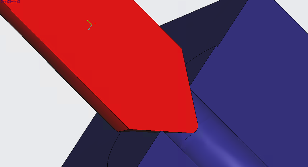
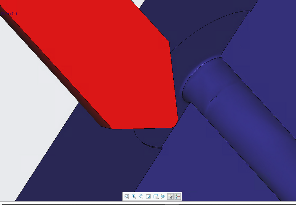
I am working on a spring pin connection to a pcb device. There are two cases in question an both applies this problem the first is when perfect alignment to the via hole occurs. For this case deformation should occur on the edges that the pin contacts the pc yet instead of that overlapping between both assemblies occurs. On the other case the alignment is not with the via but instead only on the plating (similar to an indentation process ) but the pin tip also instead of penetrating and deforming the surfaces the results show overlapping once again
Solved! Go to Solution.
- Labels:
-
General
Accepted Solutions
- Mark as New
- Bookmark
- Subscribe
- Mute
- Subscribe to RSS Feed
- Permalink
- Notify Moderator
The contact force will be determined by Hooke's law for the spring if the deflection is within the stroke of the spring. You can do this manually much faster than using Creo to calculate the force. If you are doing this as an academic exercise then put the pin at a set location and then measure the reaction force in the spring. Make sure the spring is constrained to the ground body on one end.
The contact area (at nominal ideal conditions) can be found by using assembly constraints that reproduce the actual contact between the parts. Try using the tangent constraint on the spherical tip or cone of the pin contacting the via pad/opening as appropriate. How are you determining the resistance as a function of contact area? I am curious if your application is so sensitive that you are worried about the contact area influencing the circuit behavior. Without simulating deformation of the components you are looking at a point or line contact with ideal geometry so no surface area available for measure in the CAD model.
If this situation is gold on gold contact then you are generally good at 50 grams force at the interface.
Involute Development, LLC
Consulting Engineers
Specialists in Creo Parametric
- Mark as New
- Bookmark
- Subscribe
- Mute
- Subscribe to RSS Feed
- Permalink
- Notify Moderator
Need more information on exactly what the Creo problem is. I am familiar with PCB manufacturing and use of pogo pins for contact and I do not understand from your description what the issue is. Post some pictures and models if possible to clarify.
What type of analysis are you attempting?
Involute Development, LLC
Consulting Engineers
Specialists in Creo Parametric
- Mark as New
- Bookmark
- Subscribe
- Mute
- Subscribe to RSS Feed
- Permalink
- Notify Moderator
Hi
So i am studying the following situations
The goal is to obtain the contact area and contact force when the docking process occurs and also have a understanding where the contact occurs on the via.
I am using a static analysis and applied a force on top of the pogo and fixated the board. I also used a symmetry constrain to speed up the problem
For the materials i used elastic-platic regime for each layer the
My problem is that as it can be seen the surfaces overlap when contact occurs instead of deforming it
I don't really know if i can share the model but if any other questions pls tell me
Thanks
- Mark as New
- Bookmark
- Subscribe
- Mute
- Subscribe to RSS Feed
- Permalink
- Notify Moderator
The contact force will be determined by Hooke's law for the spring if the deflection is within the stroke of the spring. You can do this manually much faster than using Creo to calculate the force. If you are doing this as an academic exercise then put the pin at a set location and then measure the reaction force in the spring. Make sure the spring is constrained to the ground body on one end.
The contact area (at nominal ideal conditions) can be found by using assembly constraints that reproduce the actual contact between the parts. Try using the tangent constraint on the spherical tip or cone of the pin contacting the via pad/opening as appropriate. How are you determining the resistance as a function of contact area? I am curious if your application is so sensitive that you are worried about the contact area influencing the circuit behavior. Without simulating deformation of the components you are looking at a point or line contact with ideal geometry so no surface area available for measure in the CAD model.
If this situation is gold on gold contact then you are generally good at 50 grams force at the interface.
Involute Development, LLC
Consulting Engineers
Specialists in Creo Parametric
- Mark as New
- Bookmark
- Subscribe
- Mute
- Subscribe to RSS Feed
- Permalink
- Notify Moderator
Hi
Thanks once again for the response
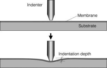
As for your suggestion about adding a tangential constrain i think that for the first case it worked. Yet for the second case what would u recommend to the second case where the pin is directly in contact with the pad. I am expecting a situation similar to hardness indentation
As for relating CRES to contact area i am also still not sure how will I do it but is a supposed scope of the project
Thanks


